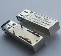
兼容光模块

Avago HFBR-5963ALZ光模块
Specifications
- 产品型号: HFBR-5963ALZ(替换型号:FTAF-M1302-02xx)
- 兼容品牌: 安华高Avago
- 封装类型: SFF2X5
- 传输速率: 155M
- 传输距离: 2KM
- 发射波长: 1300nm
- 接收波长: 1300nm
- 工作温度: 商业级0℃~+70℃/工业级-40℃~+85℃ 可选
- 数字诊断: 不带DDM
- 接收灵敏度: Avago HFBR-5963ALZ光模块
- 接收灵敏度: Avago HFBR-5963ALZ光模块
Description
产品型号:(Avago:HFBR-5963ALZ(替换型号:FTAF-M1303-02xx))
产品描述:SFF2x5-1300nm-155M-3.3V-Data:LVPECL-SD:LVTTL-LC
兼容品牌:Avago
原厂描述:SFF2x5-1300nm-155M-3.3V-Data:LVPECL-SD:LVTTL-LC
Multimode Small Form Factor Transceivers for ATM, FDDI,Fast Ethernet and SONET OC-3/SDH STM-1 with LC Connector
Description
The HFBR-5963xxZ transceiver provides the system designer with a product to implement a range of solutions for multimode fber Fast Ethernet and SONET OC-3 (SDH STM-1) physical layers for ATM and other services.
This transceiver is supplied in the industry standard 2 x5 DIP style with an LC fber connector interface with an external connector shield.
Applications
SONET/SDH equipment interconnect, OC-3/SDH STM-1 rate
Fast Ethernet
Multimode fber ATM backbone links
Features
RoHS compliant
Multisourced 2 x 5 package style
Operates with 62.5/125 mm and 50/125 mm multimode fber
Single +3.3 V power supply
Wave solder and aqueous wash process compatibility
Manufactured in an ISO 9001 certifed facility
Full compliance with ATM Forum
UNI SONET OC-3 multimode fber physical layer specifcation
Full compliance with the optical performance requirements of the FDDI PMD standard
Full compliance with the optical performance requirements of 100Base-FX version of IEEE802.3u
+3.3 V TTL signal detect output
Temperature range:
0 °C to +70 °C HFBR-5963LZ
-40 °C to +85 °C HFBR-5963ALZ
The transmitter section of the HFBR-5963xxZ utilizes a 1300 nm InGaAsP LED. This LED is packaged in the optical
subassembly portion of the transmitter section. It is driven by a custom silicon IC which converts differential PECL logic signals, ECL referenced (shifted) to a +3.3 V
supply, into an analog LED drive current.
The receiver section of the HFBR-5963xxZ utilizes an InGaAs PIN photodiode coupled to a custom silicon tran simpedance preamplifer IC. It is packaged in the optical
subassembly portion of the receiver.This PIN/preamplifer combination is coupled to a custom quantizer IC which provides the fnal pulse shaping for
the logic output and the signal detect function. The data output is differential. The data output is PECL compatible, ECL referenced (shifted) to a +3.3 V power supply.
The receiver outputs, data output and data out bar, are squelched at signal detect deassert. The signal detect output is single ended. The signal detect circuit works by sensing the level of the received signal and comparing this level to a reference. The SD output is +3.3 V TTL.
Performance figures, data and any illustrative material provided in this data sheet are typical and must be specifically confirmed in writing by F-tone Networks before they become applicable to any particular order or contract. In accordance with the F-tone Networks policy of continuous improvement specifications may change without notice.
The publication of information in this data sheet does not imply freedom from patent or other protective rights of F-tone Networks or others. Further details are available from any F-tone Networks sales representative.

