标准光模块

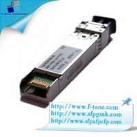
SFP+ 850nm多模光模块
Specifications
- 产品型号: FTCS-851X-02X
- 兼容品牌: 全系列
- 封装类型: SFP+
- 传输速率: Supports 9.95Gbps to 10.5Gbps bit rates
- 传输距离: 传输距离300米
- 发射波长: 850nm
- 接收波长: 850nm
- 工作温度: 商业级0℃~+70℃/工业级-40℃~+85℃ 可选
- 数字诊断: 带DDM
- 接收灵敏度: 传输距离300米
- 接收灵敏度: 传输距离300米
Description
SFP+ SR Optical Transceiver
1/10Gbps 850nm Multimode Datacom SFP+ Optical Transceiver
Features
- Hot-pluggable SFP+ footprint
- Supports rate selectable 1.25 Gb/sOr 9.95 to 10.3 Gb/s bit rates
- Power dissipation < 1W
- RoHS-6 compliant ( lead-free )
- Single 3.3V power supply
- Maximum link length of 300m on2000 MHZ-km MMF
- Uncooled 850nm VCSEL laser
- Receiver limiting electrical interface
- Duplex LC Connector
- Built-in digital diagnostic functions
- Commercial temperature range: 0°C to 70°C(Standard), -40°C to 85°C (Industrial)
Applications
- 1000BASE-SX 1G Ethernet
- 10GBASE-SR/SW 10G Ethernet
- Other optical links
Product description
F-tone’sFTCS-851X-02X 1G/10G Dual-Rate SFP+ transceivers are designed for use in 1-Gigabit and 10-Gigabit Ethernet links over multimode fiber. They are compliant with SFF-8431, IEEE 802.3-2005 10GBASE-SR/SW and 1000BASE-SX. Digital diagnostics functions are available via a 2-wire serial interface, as specified in SFF-8472. The FTCS-851X-02X is a “limiting module”, i.e., it employs a limiting receiver. Host board designers using an EDC PHY IC should follow the IC manufacturer’s recommended settings for interoperability with an SFP+ limiting module. This product is for applications specifically designed for 10G SFP+ ports and 1G/10G SFP+ ports and not native 1G SFP ports. The transceiver is RoHS compliant and lead free per Directive 2002/95/EC5.
Absolute Maximum Ratings
These values represent the damage threshold of the module. Stress in excess of any of the individual Absolute Maximum Ratings can cause immediate catastrophic damage to the module even if all other parameters are within Recommended Operating Conditions.
|
Parameters |
Symbol |
Min. |
Max. |
Unit |
|
Supply Voltage |
VCC |
-0.5 |
+3.6 |
V |
|
Storage Temperature |
Tc |
-40 |
+85 |
°C |
|
Operating Case Temperature |
Tc |
0 |
+70 |
°C |
|
Relative Humidity |
RH |
0 |
85 |
% |
Table 3: Absolute Maximum Rating
Recommended Operating Conditions
|
Parameter |
Symbol |
Min. |
Typical |
Max |
Unit |
|
Supply Voltage |
VCC |
3.0 |
3.3 |
3.6 |
V |
|
Supply current |
Icc |
200 |
300 |
mA |
|
|
Operating Case Temperature |
TC |
0 |
25 |
70 |
°C |
|
Module Power Dissipation |
Pm |
- |
0.7 |
1 |
W |
Notes:
[1] Supply current is shared between VCCTX and VCCRX.
[2] In-rush is defined as current level above steady state current requirements.
Electrical characteristics(TOP = 0 to 70℃, VCC = 3.14 to 3.46 Volts)
|
Parameter |
Symbol |
Min. |
Typical |
Max |
Unit |
Ref. |
|
Supply Voltage |
VCC |
3.14 |
3.46 |
V |
||
|
Supply Voltage |
Icc |
250 |
mA |
|||
|
Transmitter |
||||||
|
Input differential impedance |
Rin |
100 |
Ω |
1 |
||
|
Differential data input swing |
Vin,pp |
180 |
700 |
mVpp |
2 |
|
|
Transmit Disable Voltage |
VD |
2 |
VCC |
V |
||
|
Transmit Enable Voltage |
VEN |
Vee |
Vee+0.8 |
V |
||
|
Receiver |
||||||
|
Output differential impedance |
Rout |
100 |
Ω |
|||
|
Differential data output swing |
Vout,pp |
300 |
700 |
mV |
3 |
|
|
Data output rise time, fall time |
tr |
28 |
ps |
4 |
||
|
LOS Fault |
VLOS fault |
2 |
VCCHOST |
V |
5 |
|
|
LOS Normal |
VLOS norm |
Vee |
Vee+0.8 |
V |
5 |
|
|
Power Supply Noise Tolerance |
VccT/VccR |
Per SFF-8431 Rev 3.0 |
mVpp |
6 |
||
Notes:
1. Connected directly to TX data input pins. AC coupling from pins into laser driver IC.
2. Voltage swing for 1G operation is equivalent to voltage swing in 10G operation (SFF-8431 Rev3.0).
3. Into 100Ω differential termination. Voltage swing for 1G operation is equivalent to voltage swing in 10G operation (SFF-8431 Rev 3.0).
4. 20–80%. Measured with Module Compliance Test Board and OMA test pattern. Use of four 1’sand four 0’s in sequence in the PRBS^9 is an acceptable alternative. SFF-8431 Rev 3.0
5. LOS is an open collector output. Should be pulled up with 4.7kΩ – 10kΩ on the host board.
Normal operation is logic 0; loss of signal is logic 1. Maximum pull-up voltage is 5.5V.
6. Testing methodology per SFF-8431. Rev 3.0
Optical characteristics for RS0 = LOW (1G Operation)
(TOP = 0 to 70℃, VCC = 3.14 to 3.46 Volts)
|
Parameter |
Symbol |
Min. |
Typical |
Max |
Units |
Ref. |
|
Transmitter |
||||||
|
Average Launch Power |
PAVE |
-9.5 |
-1 |
dBm |
1 |
|
|
Optical Wavelength |
λC |
840 |
850 |
860 |
nm |
2 |
|
Rise-Fall Time |
Trise/Tfall |
0.26 |
ns |
3 |
||
|
RMS Spectral Width |
Δλrms |
0.45 |
dB |
|||
|
Average Extinction Ratio |
ER |
9 |
dB |
|||
|
Average Launch Power of OFF Transmitter |
POFF |
-30 |
dBm |
|||
|
Eye Mask |
Compliant with IEEE 802.3 |
|||||
|
Tx Jitter |
Txj |
|||||
|
Relative Intensity Noise |
RIN |
-117 |
dB/Hz |
|||
|
Receiver |
||||||
|
Wavelength Range |
λC |
840 |
860 |
Nm |
2 |
|
|
Receiver Sensitivity |
RSENS |
-17 |
dBm |
|||
|
Stressed Receiver Sensitivity 50 μm MMF |
SRS50um |
-13.5 |
dBm |
4 |
||
|
Stressed Receiver Sensitivity 62.5 μm MMF |
SRS62um |
-12.5 |
dBm |
4 |
||
|
Maximum Input Power |
PMAX |
+0.5 |
dBm |
|||
|
Return Loss |
Rrx |
12 |
dB |
|||
|
LOS De-Assert |
LOSD |
-18 |
dBm |
|||
|
LOS Assert |
LOSA |
-30 |
dBm |
|||
|
LOS Hysteresis |
0.5 |
dB |
||||
Notes:
1. Max is equivalent to 10G max spec.
2. This product has not been designed to support 780-nm laser operation.
3. 20%-80%.
4. Per IEEE 802.3-2005. 9dB extinction ratio transmitter.
Optical characteristics for RS0 = HIGH (10G Operation)
(TOP = 0 to 70℃, VCC = 3.14 to 3.46 Volts)
|
Parameter |
Symbol |
Min. |
Typical |
Max |
Units |
Ref. |
|
Transmitter |
||||||
|
Average Modulation Amplitude(OMA) |
POMA |
-1.5 |
dBm |
1 |
||
|
Average Launch Power |
PAVE |
-5 |
-1 |
dBm |
2 |
|
|
Optical Wavelength |
λC |
840 |
850 |
860 |
nm |
1 |
|
RMS Spectral Width |
Δλrms |
0.45 |
dB |
1 |
||
|
Average Extinction Ratio |
ER |
3.5 |
dB |
|||
|
Average Launch Power of OFF Transmitter |
POFF |
-30 |
dBm |
|||
|
Eye Mask |
Compliant with IEEE 802.3 |
|||||
|
Tx Jitter |
Txj |
|||||
|
Relative Intensity Noise |
RIN |
-117 |
dB/Hz |
|||
|
Receiver |
||||||
|
Wavelength Range |
λC |
840 |
860 |
Nm |
||
|
Receiver Sensitivity(OMA)@10.3Gb/s |
RSENS1 |
-11.1 |
dBm |
3 |
||
|
Stressed Receiver Sensitivity (OMA) @ 10.3Gb/s |
RSENS2 |
-7.5 |
dBm |
4 |
||
|
Maximum Input Power |
PMAX |
+0.5 |
dBm |
|||
|
Return Loss |
Rrx |
12 |
dB |
|||
|
LOS De-Assert |
LOSD |
-18 |
dBm |
|||
|
LOS Assert |
LOSA |
-30 |
dBm |
|||
|
LOS Hysteresis |
0.5 |
dB |
||||
Notes:
1. Per Tradeoff Table 52.8, IEEE 802.3-2005
2. Average Power figures are informative only, per IEEE802.3-2005.
3. Measured with worst ER; BER<10-12; 231 – 1 PRBS.
4. Per IEEE 802.3-2005.
General Specifications
|
Parameter |
Symbol |
Min. |
Typical |
Max |
Units |
Ref. |
|
Bit Rate (RS0 = LOW) |
BR |
1.25 |
Gb/s |
1 |
||
|
Bit Rate (RS0 = HIGH) |
BR |
9.95 |
10.3 |
Gb/s |
2 |
|
Parameter |
Symbol |
Max. Supported Distance |
Units |
||
|
Distance |
@1G |
@10G |
|||
|
Fiber Type |
850nm OFL Bandwidth |
||||
|
62.5µm |
160 MHz-km |
Lmax |
220 |
26 |
m |
|
275 |
33 |
||||
|
50µm |
400 MHz-km |
Lmax |
500 |
66 |
m |
|
OM2 500 MHz-km |
550 |
82 |
|||
|
OM3 2000 MHz-km |
>550 |
300 |
|||
Notes:
1. 1000BASE-SX. Tested with a 27 – 1 PRBS. See Section I, Note 5 for RS0 conditions for 1.25Gb/s operation.
2. 10GBASE-SR/SW. Tested with a 231 – 1 PRBS. See Section I, Note 5 for RS0 conditions for 10.3 Gb/s operation.
Pin Descriptions
Figure1.Electrical Pin-out Details
|
Pin |
Symbol |
Name/Description |
|
1 |
VEET [1] |
Transmitter Ground |
|
2 |
Tx_FAULT [2] |
Transmitter Fault |
|
3 |
Tx_DIS [3] |
Transmitter Disable. Laser output disabled on high or open |
|
4 |
SDA [2] |
2-wire Serial Interface Data Line |
|
5 |
SCL [2] |
2-wire Serial Interface Clock Line |
|
6 |
MOD_ABS [4] |
Module Absent. Grounded within the module |
|
7 |
RS0 [5] |
RS0 for Rate Select: Open or Low = Module supports ≤4.25Gbps High = Module supports 9.95 Gb/s to 10.3125 Gb/s |
|
8 |
RX_LOS [2] |
Loss of Signal indication. Logic 0 indicates normal operation |
|
9 |
RS1 [5] |
No connection required |
|
10 |
VEER [1] |
Receiver Ground |
|
11 |
VEER [1] |
Receiver Ground |
|
12 |
RD- |
Receiver Inverted DATA out. AC Coupled |
|
13 |
RD+ |
Receiver DATA out. AC Coupled |
|
14 |
VEER [1] |
Receiver Ground |
|
15 |
VCCR |
Receiver Power Supply |
|
16 |
VCCT |
Transmitter Power Supply |
|
17 |
VEET [1] |
Transmitter Ground |
|
18 |
TD+ |
Transmitter DATA in. AC Coupled |
|
19 |
TD- |
Transmitter Inverted DATA in. AC Coupled |
|
20 |
VEET [1] |
Transmitter Ground |
Notes:
[1] Module circuit ground is isolated from module chassis ground within the module.
[2].should be pulled up with 4.7k – 10k ohms on host board to a voltage between 3.15Vand 3.6V.
[3]Tx_Disable is an input contact with a 4.7 kΩ to 10 kΩ pullup to VccT inside the module.
[4]Mod_ABS is connected to VeeT or VeeR in the SFP+ module. The host may pull this contact up to Vcc_Host with a resistor in the range 4.7 kΩ to10 kΩ.Mod_ABS is asserted “High” when the SFP+ module is physically absent from a host slot.
[5]RS0 and RS1 are module inputs and are pulled low to VeeT with > 30 kΩ resistors in the module.
Ordering information
|
Part Number |
Product Description |
|
FTCS-851X-02 |
850nm, 10Gbps, 300m, 0ºC ~ +70ºC |
|
FTCS-851X-02I |
850nm, 10Gbps, 300m, -40°C to 85°C (Industrial) |


