标准光模块

兼容安华高AFBR-5803AZ
Description
兼容安华高AFBR-5803AZ
Product Features
● Uncooled laser diode with MQW structure
● Reach 2 km Transmission Distance
● Duplex Single Mode Transceiver 1x9 Footprint
● SC, FC or ST Optical Interface are Optional
● Single +3.3V Power Supply
● PECL/LVPECL Differential Inputs and Outputs
● PECL/LVPECL Signal Detection Output alternative
● Fast Ethernet and ITU G.957 Compliant
● Compliant RoHS and lead free
● Complies with Telcordia GR-468-CORE
● Operating case temperature:
Standard : 0 to +70℃
Extend : -20 to +85℃
Industrial : -40 to +85℃
Product Applications
● ATM
● SONET/SDH
● Fast Ethernet
● Switches
● Routers
● Hubs
Performance Specifications
Absolute Maximum Ratings
|
Parameter |
Symbol |
Min |
Max |
Unit |
|
|
Storage Temperature |
Tst |
-40 |
+85 |
℃ |
|
|
Operating Temperature |
TO |
FTBR-5803Z/FTBR-5803TZ |
0 |
+70 |
℃ |
|
FTBR-5803AZ/FTBR-5803ATZ |
-20 |
+85 |
℃ |
||
|
FTBR-5803AQZ/FTBR-5803ATQZ |
-40 |
+85 |
℃ |
||
|
Input Voltage |
- |
GND |
VCC |
V |
|
|
Power Supply Voltage |
VCC-VEE |
0 |
+6 |
V |
|
Recommended Operating Conditions
|
Parameter |
Symbol |
Min |
Typ |
Max |
Unit |
|
|
Storage Temperature |
Tst |
-40 |
- |
+85 |
℃ |
|
|
Operating Case Temperature |
TC |
FTBR-5803Z/FTBR-5803TZ |
0 |
- |
+70 |
℃ |
|
FTBR-5803AZ/FTBR-5803ATZ |
-20 |
- |
+85 |
℃ |
||
|
FTBR-5803AQZ/FTBR-5803ATQZ |
-40 |
- |
+85 |
℃ |
||
|
Power Supply Voltage |
VCC3.3 |
3.1 |
3.3 |
3.5 |
V |
|
|
Data Rate |
DR |
- |
155 |
200 |
Mbps |
|
Optical Specification
|
Transmitter |
|||||||
|
Parameter |
Symbol |
Min |
Typ |
Max |
Unit |
Note |
|
|
Center Wavelength |
1310 FP |
lC |
1261 |
1310 |
1360 |
nm |
FTBR-5803xx |
|
1550 FP |
1500 |
1550 |
1600 |
FTBR-5803xx-1550nm |
|||
|
Spectral Width |
Dl |
- |
- |
4 |
nm |
- |
|
|
Average Optical Output Power |
Po |
-20 |
- |
-14 |
dBm |
62.5/125UM MMF |
|
|
Average Optical Output Power |
Po |
-22.5 |
|
-14 |
dBm |
50/125UM MMF |
|
|
Extinction Ratio |
Ext |
10 |
- |
- |
dB |
- |
|
|
Optical Rise Time(20%-80%) |
Tr |
- |
- |
3 |
ns |
- |
|
|
Optical Fall Time(20%-80%) |
Tf |
- |
- |
3 |
ns |
- |
|
|
Output Eye Diagram |
Compliant with ITU-T.G957 |
||||||
|
Receiver |
|||||||
|
Parameter |
Symbol |
Min |
Typ |
Max |
Unit |
Note |
|
|
Operate Wavelength |
- |
1261 |
- |
1620 |
nm |
- |
|
|
Sensitivity |
Pr |
- |
- |
-32 |
dBm |
1 |
|
|
Saturation |
Ps |
-3 |
- |
- |
dBm |
1 |
|
|
Signal Detect Assert Level |
- |
-45 |
- |
- |
dBm |
Alarm: Low-level |
|
|
Signal Detect De-assert Level |
- |
- |
- |
-33 |
dBm |
||
|
SD Hysteresis |
- |
0.5 |
- |
5 |
dB |
- |
|
Note: 1. Minimum Sensitivity and saturation levels for a 2 23 -1 PRBS test pattern @155Mbps.
Electrical Specification
|
Transmitter |
||||||
|
Parameter |
Symbol |
Min |
Typ |
Max |
Unit |
Note |
|
Power Supply Current |
ICC |
- |
70 |
120 |
mA |
2 |
|
Input Differential Impedance |
ZIN |
90 |
100 |
110 |
Ω |
- |
|
Differential Input Voltage |
VIH- VIL |
300 |
- |
2000 |
mV |
- |
|
Receiver |
||||||
|
Parameter |
Symbol |
Min |
Typ |
Max |
Unit |
Note |
|
Power Supply Current |
ICC |
- |
60 |
80 |
mA |
2 |
|
Data Output Voltage-Low |
VOL-VCC |
-2.0 |
- |
- 1.58 |
V |
3 |
|
Data Output Voltage-High |
VOH-VCC |
- 1.1 |
- |
-0.74 |
V |
3 |
|
Signal Detect Output Voltage-Low |
VSDL-VCC |
-2.0 |
- |
- 1.58 |
V |
PECL |
|
Signal Detect Output Voltage-High |
VSDH-VCC |
- 1.1 |
- |
-0.74 |
V |
|
Note: 2. The current excludes the output load current.
3. Terminated with 50Ohm to Vcc-2V.
Pin Definitions
PIN Diagram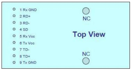
PIN Description
|
PIN |
Symbol |
Note |
|
1 |
GNDR |
Directly connect this pin to receiver signal ground plane. |
|
2 |
RD+ |
See recommended circuit schematic. |
|
3 |
RD- |
See recommended circuit schematic. |
|
4 |
SD |
Active high on this indicates a receiver optical signal. |
|
5 |
VCCR |
+3.3V DC power for the receiver section. |
|
6 |
VCCT |
+3.3V DC power for the transmitter section. |
|
7 |
TD- |
See recommended circuit schematic. |
|
8 |
TD+ |
See recommended circuit schematic. |
|
9 |
GNDT |
Directly connect this pin to transmitter signal ground plane. |
Recommended Circuit 1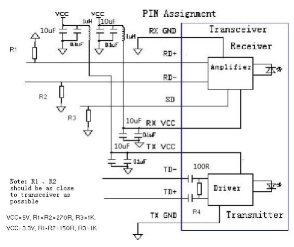
Recommended Circuit 2
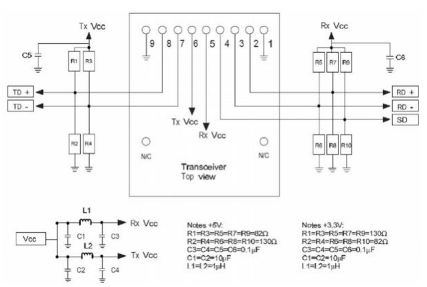
Note: The split-loaded terminations for ECL signals need to be located at the input of devices receiving those ECL signals. The power supply filtering is required for good EMI performance.Use short tracks from the inductors L1/L2 to the module Rx VCC/Tx VCC. A GND plane under the module is required for good EMI and sensitivity performance
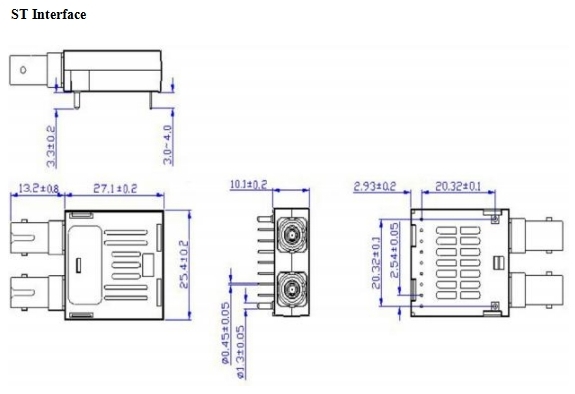
Package Diagram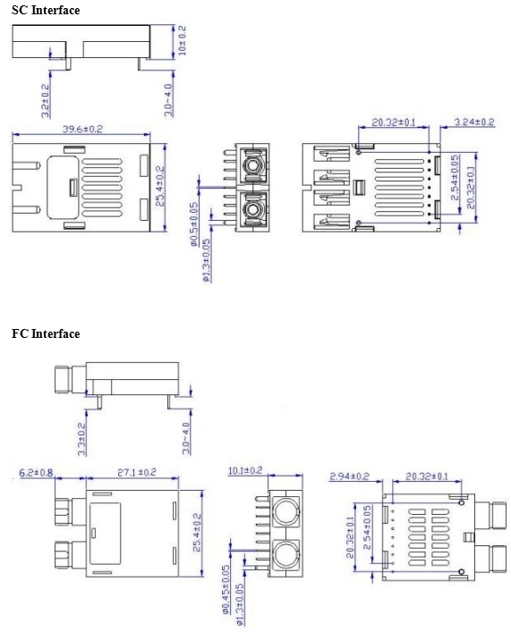
Order Information
|
FTBR-5803Z |
兼容AVAGO(安华高)AFBR-5803Z,国产替换兼容AVAGO(安华高)AFBR-5803Z |
|
FTBR-5803TZ |
兼容AVAGO(安华高)AFBR-5803TZ,国产替换兼容AVAGO(安华高)AFBR-5803TZ |
|
FTBR-5803AZ |
兼容AVAGO(安华高)AFBR-5803AZ,国产替换兼容AVAGO(安华高)AFBR-5803AZ |
|
FTBR-5803ATZ |
兼容AVAGO(安华高)AFBR-5803ATZ,国产替换兼容AVAGO(安华高)AFBR-5803ATZ |
|
FTBR-5803AQZ |
兼容AVAGO(安华高)AFBR-5803AQZ,国产替换兼容AVAGO(安华高)AFBR-5803AQZ |
|
FTBR-5803ATQZ |
兼容AVAGO(安华高)AFBR-5803ATQZ,国产替换兼容AVAGO(安华高)AFBR-5803ATQZ |
其他还有大量可替换avago finisar ....等等品牌的产品,请联系北亿纤通的市场人员
Important Notice
Performance figures, data and any illustrative material provided in this data sheet are typical and must be specifically confirmed in writing by F-tone Networks before they become applicable to any particular order or contract. In accordance with the F-tone Networks policy of continuous improvement specifications may change without notice.
The publication of information in this data sheet does not imply freedom from patent or other protective rights of F-tone Networks or others. Further details are available from any F-tone Networks sales representative.


